Machinability Enhancement of Lead-Free Brass Alloys
2020-05-31
Abstract
This paper deals with fundamental investigations on the machinability of lead-free brass alloys. The effect of microstructure and silicon as alloying element on chip formation, cutting forces, tool temperatures and tool wear is analyzed during external turning. Based on that, various approaches for machinability enhancement were investigated in order to enable high performance cutting operations. The paper focuses on the influence of various tool coatings such as TiB2, DLC and diamond on abrasive and adhesive tool wear. Besides a significant decrease of tool wear, dry turning of lead-free brass alloys was realized by adapted tool coating. Moreover, investigations on the performance of PCD tools as well as high-pressure coolant supply strategy were carried out.
1.Introduction
Brass alloys are characterized by high thermal and electric conductivity as well as outstanding antibacterial properties and are therefore widely used in various industries such as electric and electronics, automotive and sanitary industry. Due to a high amount of cutting operations when manufacturing brass components, different alloying elements enhancing the machinability are usually added to brass. The most important element in this context is lead, improving the machinability with regard to excellent chip breakage, low tool wear and high applicable cutting parameters. These aspects can be explained by two basic phenomena. First of all, solubility of lead in brass is very low and consequently, lead segregates in the entire microstructure, particularly at the grain boundaries. Hence, shear strength is significantly reduced, resulting in very good chip breakage. Secondly, lead exhibits a low melting temperature of Tm = 327.5 °C. During cutting, a thin, semifluid lead film reduces friction and thereby, cutting forces and tool wear.
However, in recent years the legislation on protecting health and environment has been tightened worldwide. The use of lead in copper alloys has been restricted as lead is a hazardous heavy metal. Depending on country and application, a maximum lead content of 0.1 % (Directive 2011/55/EU [RoHS], Directive 2000/53/EC [ELV]) to 0.25 % (Safe Drinking Water Act, USA) in copper alloys was prescribed. Up to now, exceptional rules are still valid in many cases (e.g. RoHS, ELV), permitting a lead content of 4 % in copper alloys. However, the necessity of these exceptional rules is checked by politics in certain periods. The machinability of lead-free brasses is significantly worse compared to leaded alloys due to the formation of long chips and reduced tool life, leading to low productivity and process stability. In the past, it was found that adding selenium and bismuth as well as graphite improves machinability of lead-free brasses.
However, the manufacturing process of the materials is very complex and cost-intensive. Moreover, bismuth is only available in limited quantities. The use of these materials is therefore not practicable in mass production. Most of the investigations on commercially available lead-free brass alloys were carried out more than twenty years ago. Driven by changed legislation, new lead-free brass alloys were developed in recent years meeting the legally prescribed requirements on maximum lead content. In previous research work the machinability of these materials © 2014 Published by Elsevier B.V. Open access under CC BY-NC-ND license. Selection and peer-review under responsibility of the International Scientific Committee of the 6th CIRP International Conference on High Performance Cutting has not been investigated in a systematical and comprehensive way. In this paper, the effect of microstructure and silicon as alternative alloying element of today’s commercially available lead-free brass alloys on machinability is therefore analyzed. Based on that, various approaches for machinability enhancement were investigated in order to enable high performance cutting operations, particularly for mass production.
2. Workpiece Materials
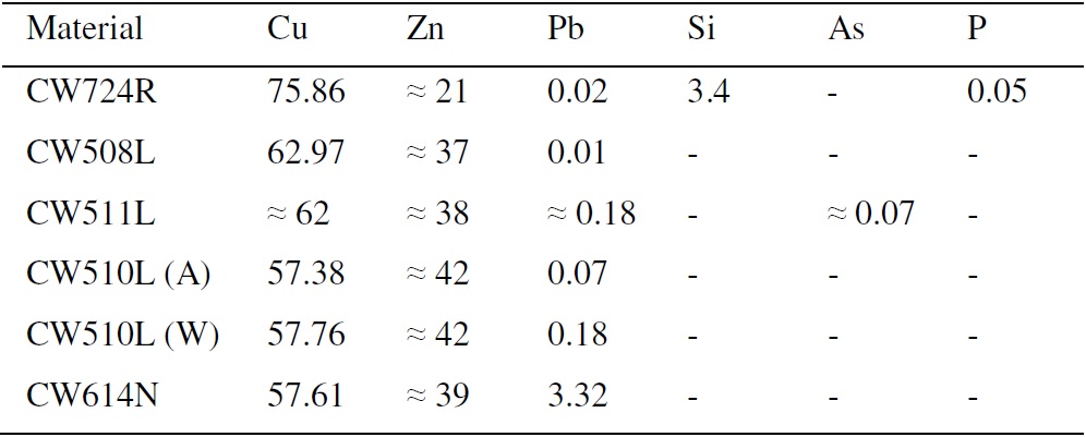
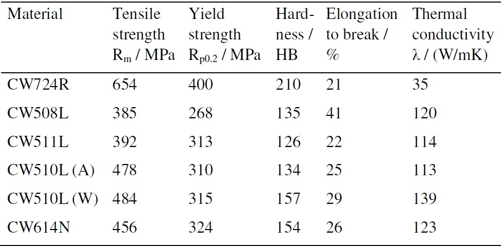
The machinability of lead-free brass alloys CW508L, CW511L and CW510L as well as silicon alloyed special brass CW724R were investigated and compared to the machinability of leaded brass CW614N (nomenclature: EN code). All materials were manufactured by continuous casting, bar extrusion (warm) and pultrusion (cold). The materials’ chemical composition is summarized in table 1. Primarily decisive for microstructure and hence, machinability, is the percentage of copper and zinc, respectively. In general, brass alloys having a zinc content of up to 37.5% consist almost solely of α-phases. Lattice structure of these α-phases is face-centered cubic (fcc) and therefore, brasses with high amount of α-phase possess a low hardness and high ductility. This applies for the alloys CW508L and CW511L with α-phase content of 90 to 98%, see fig. 1 and table 2. Huge difference between these two materials is the remaining lead content of 0.01% (CW508L) and 0.18 % (CW511L), table 1. Increasing the content of zinc over 38 % results in an increased percentage of β-phase. The material CW510L consists of 42% zinc and hence, the content of α- and β-phase is nearly balanced, see fig. 1 (d) and (e). The β-phase possesses a body-centered cubic (bcc) lattice and is much harder and less formable than the α-phase. Therefore, hardness and tensile strength of CW510L is higher compared to CW508L and CW511L, see table 2. In this study, two different CW510L alloys were investigated, differing in the lead content of Pb = 0.07% (CW510L (A)) and 0.18% (CW510L (W)) in order to analyze the effect of different remaining lead contents.
Table 1: Chemical composition of the workpiece materials
The leaded brass CW614N possessed 39 % zinc and 3.32 % lead, resulting in a microstructure of 70 % α-phase and 30% β-phase. Lead is almost not soluble in brass and segregates mainly at grain boundaries, see fig. 1 (f). Hence, shear strength is significantly reduced, whereas elongation to break is similar to lead-free brass alloys, table 2. CW724R is a recently developed special brass that was alloyed with 3.4 % of silicon. Due to a low zinc content of 21 %, the material possesses a high percentage of α-phase of approximately 60 %. Besides, a silicon-rich, brittle and highly abrasive k-phase exits in the microstructure, leading to a high hardness and tensile strength of the material, table 2. Moreover, intermetallic compounds (γ-phases) are segregated at the grain boundaries, fig. 1 (a).
%20CW724R%20(b)%20CW508L.jpg)
Fig. 1: Cross sections of the microstructure of (a) CW724R; (b) CW508L; (c) CW511L; (d) CW510L (A); (e) CW510L (W); (f) CW614N
Table 2: Thermo mechanical properties of the workpiece materials
3. Effect of Microstructure and Alloying Elements on Machinability
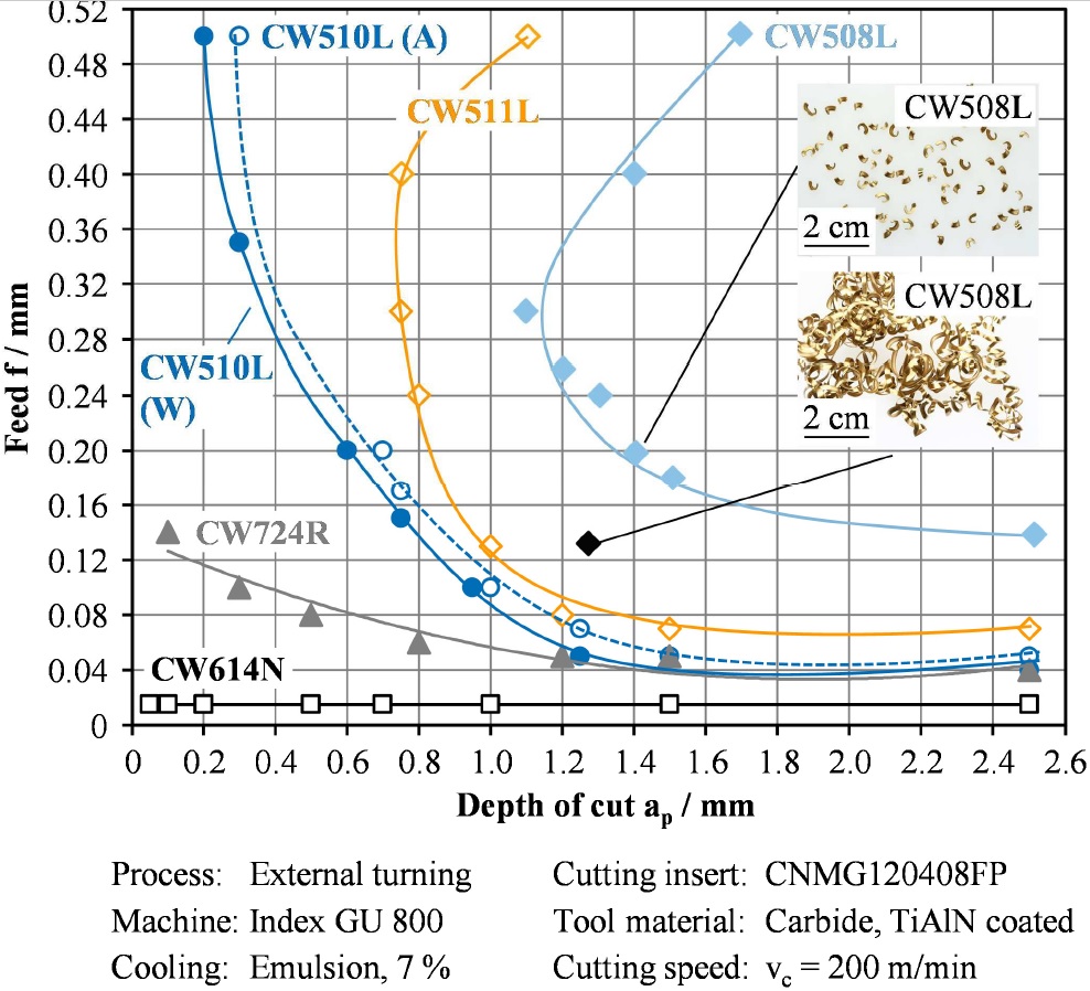
The machinability of different lead-free brass alloys was investigated in external turning experiments on a CNC lathe Index GU 800, section 3.1, 3.2, as well as on an automatic lathe Traub TNS 42, section 3.3. All experiments were carried out under wet conditions (emulsion Jokisch Universal W5 RW TH, 7 %), using mainly carbide cutting inserts. Different cutting parameters, tool geometries and coatings were applied for roughing and finishing conditions. The boundary conditions are summarized in fig. 2 to 6, respectively.
3.1. Chip formation
One important factor for fully automatic mass production of brass components is high process stability through excellent chip breakage. Chip formation was investigated during external turning depending on feed f and depth of cut ap, while the cutting speed was kept constant to vc = 200 m/min. Starting from high f and ap values, the graphs in fig. 2 represent the crossover from longer chips (1-5) to exclusively loose arc chips (6.2), elemental chips (7.1) or needle chips (8.1) (classification acc. to ISO 3685:1993). Best chip breakage was determined for turning CW614N due to the positive effect of lead (Pb = 3.32 %). Independently of the cutting parameters, only needle chips (8.1) were formed. Adding silicon to brass results in the formation of brittle k-phases in the microstructure. Hence, special brass CW724R (Si = 3.4 %) showed better chip breakage than silicon-free and lead-free brasses. At most of the cutting parameters short elemental chips (7.1) were formed. However, longer chips compared to leaded CW614N were detected at low f and ap.
Amongst lead-free and silicon-free brasses, CW510L (A) and CW510L (W) showed better chip breakage than CW511L and CW508L due to a higher percentage of brittle bcc β- phase, fig. 2. Depending on the cutting parameters, the formation of elemental (7.1) or tubular chips (2.1/2.2) was observed. CW510L (W), possessing a lead content of Pb = 0.18 %, showed slightly better chip breakage than CW510L (A) with a lead content of Pb = 0.07 %. Hence, it can be concluded that even small differences in remaining lead content affects chip formation. Worst chip breakage of all materials was determined for CW508L, caused by a high percentage of ductile fcc α-phase and, compared to CW511L, low residual lead content of Pb = 0.01 %. Both materials, CW508L and CW511L, tended to form long or snarled tubular chips (2.1/2.3). Only at relatively high f and ap, short arc or elemental chips were formed (6.2/7.1).
Amongst lead-free and silicon-free brasses, CW510L (A) and CW510L (W) showed better chip breakage than CW511L and CW508L due to a higher percentage of brittle bcc β- phase, fig. 2. Depending on the cutting parameters, the formation of elemental (7.1) or tubular chips (2.1/2.2) was observed. CW510L (W), possessing a lead content of Pb = 0.18 %, showed slightly better chip breakage than CW510L (A) with a lead content of Pb = 0.07 %. Hence, it can be concluded that even small differences in remaining lead content affects chip formation. Worst chip breakage of all materials was determined for CW508L, caused by a high percentage of ductile fcc α-phase and, compared to CW511L, low residual lead content of Pb = 0.01 %. Both materials, CW508L and CW511L, tended to form long or snarled tubular chips (2.1/2.3). Only at relatively high f and ap, short arc or elemental chips were formed (6.2/7.1).
Fig. 2: Chip breakage of brass alloys depending on feed and depth of cut
Besides chip breakage, huge differences were detected regarding the mechanism of chip formation. Fig. 3 compares longitudinal cross sections of chips generated at external turning under the same boundary conditions. Lead significantly reduces friction in the cutting zone and hence, chip thickness ratio was nearly 1 (Ȝh § 1.2) when turning leaded CW614N. In this case, the chip broke after forming the first lamella due to the material’s low shear strength. When turning silicon alloyed special brass CW724R, discontinuous chips were formed due to brittle k-phases. Chip thickness ratio and consequently friction was low (Ȝh § 1.2). However, the huge chip segmentation caused high process dynamics, which might result in chatter marks at the workpiece surface or chipping of the cutting edge. Lamellar chips were formed when turning CW510L. Due to the lacking effects of alloying elements such as lead or silicon, friction in the cutting zone is higher and therefore, a clear distortion of the microstructure at the chip’s bottom surface was observed. Again, a difference between both CW510L materials was detected, as chip thickness ratio was higher for CW510L (A) due to its lower lead content (Ȝh § 1.8 compared to 1.5). The highest distortion of the microstructure at the chip’s bottom surface was determined when turning CW508L and CW511L. Due to the big amount of ductile fcc α-phase, continuous chips were formed and high chip thickness ratios of Ȝh § 2.8 were determined for both materials.
%20CW724R.jpg)
Fig. 3: Mechanisms of chip formation when turning (a) CW724R; (b) CW508L; (c) CW511L; (d) CW510L (A); (e) CW510L (W); (f) CW614N
3.2. Thermo mechanical tool load
The different mechanisms of chip formation and friction conditions as well as mechanical properties of the materials highly affect the cutting forces and temperatures. The specific cutting forces kc1.1 at a width of undeformed chip of b = 1 mm and a thickness of undeformed chip of h = 1 mm as well as the rise of specific cutting force 1-mc were calculated acc. to Kienzle (Fc = kc1.1•b•h1-mc), see fig. 4 (a). For this purpose, cutting forces were measured during external turning by means of a 3-component Kistler platform type 9121 (filter: low pass, frequency rate: 1 kHz, sampling rate 100 Hz). The influence of the cutting edge radius (rβ= 6 microns) was negligible in the regarded feed range from f = 0.05 - 0.4 mm. Moreover, temperatures were measured on the bottom of a blind hole within the tool close to the cutting edge by using a fibre-optic two-colour pyrometer, see fig. 4 (b). The measurement point was located 0.35 mm from the major flank face, 0.15 mm from the rake face at the minimum and had a diameter of 0.5 mm.
For all measurements the same tool was used in order to prevent errors based on different blind hole positions. The influence of tool wear was negligible. All force and temperature measurements were repeated twice. For leaded brass CW614N, a specific cutting force of kc1.1 = 392 N/mm2 was calculated and a tool temperature of Tt = 182 °C was measured, fig. 4. In contrast, specific cutting forces and tool temperatures were approximately two to three times higher when turning lead-free and silicon-free brasses. Highest kc1.1-value and tool temperature were determined for CW508L (kc1.1 = 1221 N/mm2, Tt = 475 °C), even though hardness and tensile strength of the material is comparatively low, see table 2. In correlation to chip compression and distortion of the microstructure at the chip’s bottom surface shown in fig. 3, it is assumed that high cutting forces and temperature can be explained by high friction in the contact zone due to high percentage of ductile fcc α-phase and very low lead content of Pb = 0.01 %.
A high content of fccαphase also led to a high kc1.1-value and tool temperature when turning CW511L (kc1.1 = 1129 N/mm2,Tt = 455 °C). However, mainly due to a higher lead content (Pb = 0.18 %), both values are slightly lower compared to CW508L. CW510L exhibits a much higher percentage of brittle bcc β-phase and is therefore characterized by a higher hardness and strength compared to CW508L and CW511L. However, the calculated kc1.1-values were lower as friction and chip compression are reduced (CW510 (A): kc1.1 = 945 N/mm2 ; CW510 (W): kc1.1 = 852 N/mm2 ). For CW510L (W) the same applies with regard to tool temperature (Tt = 425°C), whereas tool temperature was in the same range as CW508L and CW511L during turning of CW510L (A) (Tt = 470°C). Consequently, a difference between the machinability of both CW510L materials, differing mainly in residual lead content, was identified with regard to thermo-mechanical tool load.
%20Specific%20cutting%20force%20and%20the%20rise%20of%20specific%20cutting%20force.jpg)
%20Specific%20cutting%20force%20and%20the%20rise%20of%20specific%20cutting%20force.jpg)
For all measurements the same tool was used in order to prevent errors based on different blind hole positions. The influence of tool wear was negligible. All force and temperature measurements were repeated twice. For leaded brass CW614N, a specific cutting force of kc1.1 = 392 N/mm2 was calculated and a tool temperature of Tt = 182 °C was measured, fig. 4. In contrast, specific cutting forces and tool temperatures were approximately two to three times higher when turning lead-free and silicon-free brasses. Highest kc1.1-value and tool temperature were determined for CW508L (kc1.1 = 1221 N/mm2, Tt = 475 °C), even though hardness and tensile strength of the material is comparatively low, see table 2. In correlation to chip compression and distortion of the microstructure at the chip’s bottom surface shown in fig. 3, it is assumed that high cutting forces and temperature can be explained by high friction in the contact zone due to high percentage of ductile fcc α-phase and very low lead content of Pb = 0.01 %.
A high content of fccαphase also led to a high kc1.1-value and tool temperature when turning CW511L (kc1.1 = 1129 N/mm2,Tt = 455 °C). However, mainly due to a higher lead content (Pb = 0.18 %), both values are slightly lower compared to CW508L. CW510L exhibits a much higher percentage of brittle bcc β-phase and is therefore characterized by a higher hardness and strength compared to CW508L and CW511L. However, the calculated kc1.1-values were lower as friction and chip compression are reduced (CW510 (A): kc1.1 = 945 N/mm2 ; CW510 (W): kc1.1 = 852 N/mm2 ). For CW510L (W) the same applies with regard to tool temperature (Tt = 425°C), whereas tool temperature was in the same range as CW508L and CW511L during turning of CW510L (A) (Tt = 470°C). Consequently, a difference between the machinability of both CW510L materials, differing mainly in residual lead content, was identified with regard to thermo-mechanical tool load.
Fig. 4: (a) Specific cutting force and the rise of specific cutting force; (b) tool temperature during turning of brass alloys
When comparing the tool temperature during cutting of different workpiece materials, the thermal conductivity of the material is decisive for the percentage of heat that is dissipated by the workpiece and chip and hence, by the tool. In this case, all silicon-free brass alloys were characterized by a similar heat conductivity, varying from Ȝ = 114 W/mK (CW511L) to 139 W/mK (CW510L (W)). Therefore, it is assumed that the difference in tool temperatures during turning of the investigated silicon-free brass alloys was not caused by different heat conductivity but microstructure. In contrast, the thermal conductivity of silicon-alloyed special brass CW724R is significantly lower (Ȝ = 35 W/mK), which tends to result in higher temperatures measured in the tool. However, due to a high percentage of silicon-rich k-phase and resulting low friction and chip compression, the tool temperature was lower compared to all lead-free and siliconfree brass alloys (Tt = 410°C). The same effects were crucial for a low specific cutting force of kc1.1 = 559 N/mm2. Nevertheless, in comparison to leaded CW614N, a remarkable increase of thermo-mechanical tool load can be stated.
3.3. Tool wear
In order to analyze to which extent the higher thermomechanical tool load affects tool wear, each brass alloy was machined in external turning at vc = 200 m/min, ap = 1 mm and f = 0.1 mm, using a TiAlN-coated carbide cutting insert. However, under these conditions differences in tool wear were not significant after a defined cutting time of tc = 150 min. Hence, a higher feed of f = 0.3 mm was applied for turning of some of the brass alloys in order to increase the load on the tool. After a cutting time of tc = 100 min very low tool wear could be identified at the cutting insert used for turning leaded CW614N, see fig. 5 (d). Abrasive flank wear as well as crater wear were almost not detectable. Behind the very small contact zone only a few workpiece material adhesions with high zinc percentage (acc. to EDX analysis) can be seen. Behind these adhesions, the tool’s substrate is exposed at some areas caused by impinging chips, however, that does not influence the cutting process.
%20CW724R.jpg)
%20CW724R.jpg)
Fig. 5: SEM photographs of tool wear when turning (a) CW724R; (b) CW511L; (c) CW510L (A); (d) CW614N
In contrast, after turning lead-free brass alloys CW511L and CW510L (A), strong adhesions on the flank as well as rake face are clearly visible, see fig. 5 (b) and (c). These adhesions might deteriorate surface quality of the workpiece. Moreover, adhered material might pull out particles of the coating and substrate, leading to chipping at the cutting edge. Due to this effect, the substrate is exposed at a small area of the major cutting edge at the end of corner radius after turning CW510L (A). The risk of chipping gets even higher when machining small brass components using very sharp tools. Besides adhesive tool wear, abrasive wear is increased as well after machining CW511L and CW510L (A). For both materials, a width of flank wear land in the range of VB = 40 - 50 µm was measured. The substrate was not yet exposed in these areas, though. It has to be stated that cutting time would have to be considerably increased for investigating abrasive tool wear caused by the various materials in a more detailed way. Due to the strongly brittle k-phase in silicon alloyed CW724R, the contact zone and adhesive tool wear was significantly reduced compared to CW511L and CW510L (A), see fig. 5 (a). However, the silicon rich k-phases are highly abrasive and therefore, flank wear was increased. The width of flank wear land was hardly to measure though, as coherent flaking of the coating occurred. It is assumed that flaking was mainly caused by a chemical reaction between silicon of the workpiece material, aluminum of the coating and oxygen of the atmosphere. These elements were detected by EDX analysis and led to the conclusion that aluminum silicon oxide was formed. Due to the high volume of oxides, this might have caused increased internal stress in the coating, and consequently flaking. Moreover, discontinuous chip formation, see fig. 3 (a), and resulting high process dynamics have probably intensified flaking of the coating.
An analysis of the surface quality of the workpiece is not in focus of this paper. However, it can be summarized that surface roughness after turning lead-free brasses was similar compared to leaded CW614N, whereas burr formation increased with rising ductility of the lead-free brass alloy.
4. Approaches for High-Performance Cutting of LeadFree Brass Alloys
Based on the fundamental investigations, various approaches for machinability enhancement of lead-free brass alloys were analyzed in order to enable high performance cutting operations, particularly for mass production. One important factor is the adaption of the tool material and coating system to the machining properties of each workpiece material. For this purpose, the performance of carbide cutting inserts with various coating systems and adapted chip groove design were investigated, see fig. 6. As workpiece material, CW510L (A) was chosen since this material is characterized by both higher abrasive and adhesive tool wear compared to leaded CW614N. In the field of PVD coatings, titanium aluminum nitride (TiAlN), titanium diboride (TiB2) and diamond-like carbon (DLC) were used. The DLC coating was made of hydrogen-free, tetrahedral carbon layers (ta-C) with high percentage of sp3 diamond bonds and low sp2 graphite bonds. Hence, the hardness of this coating material is higher (§ 5,000 HV0.05) compared to TiAlN (§ 3,300 HV0.05) and TiB2 (§ 4,000 HV0.05). The thickness of the used PVD coatings varied from 1 micron (DLC) to 1.7 microns (TiAlN) and 2.3 microns (TiB2). Additionally, to PVD-coatings, a diamond CVD-coating with a very high hardness (10,000 HV0.05) was applied. The experiments were conducted on an automatic lathe (Traub TNS 42) up to a cutting time of tc = 50 min at vc = 200 m/min, ap = 1 mm and f = 0.3 mm, while the tool substrate and geometry was kept constant.
%20TiAlN%3B%20(b)%20TiB2%3B%20(c)%20DLC.jpg)
%20TiAlN%3B%20(b)%20TiB2%3B%20(D)%20DLC.png)
Fig. 6: Tool wear of carbide inserts coated with (a) TiAlN; (b) TiB2; (c) DLC; (d) diamond when turning CW510L (A)
In comparison to uncoated carbide, adhesion of the workpiece material on the tool was slightly reduced by TiAlN and TiB2 coating. However, especially on the rake face of TiB2 coated tool, strong material adhesion was still clearly visible by light microscopy, see fig. 6 (b). In contrast, adhesion tendency was significantly reduced when using DLC coating. Important factors explaining the different results are surface roughness and coefficient of friction of the coating materials. In addition, it is assumed that due to a higher thermal conductivity of the DLC coating, temperatures in the cutting zone were lower which might have reduced adhesion tendency. Moreover, it is supposed that the substrate of the TiB2 coated tool was exposed on the rake face near to the cutting edge, resulting in an adhesion tendency comparable to the uncoated carbide tool. Besides adhesive wear, also abrasive wear was reduced by DLC coating compared to TiAlN and TiB2 coating, which can be mainly explained by the higher hardness and abrasion resistance of the coating material. The width of flank wear land was measured to only VB = 8 µm for DLC coating, while VB amounted 17 µm for TiAlN and 32 µm for TiB2 coating.
A further increase in cutting performance was achieved by a diamond CVD-coating. As shown in fig. 6 (d), no material adhered to the rake as well as flank face of the tool. Moreover, the hardness and abrasion resistance of the diamond coating is outstandingly high and therefore, almost no abrasive flank wear could be identified. In further experiments, diamond coated tools were successfully used in dry turning of CW510L (A). However, disadvantage of the diamond coating is a higher cutting edge roundness due to a required pretreatment of the substrate as well as a high coating thickness. The cutting edge radius of the used diamond coated inserts (coating thickness of 8 microns) was measured to r⧠15 microns. Sharp cutting edges are to be preferred in general for machining lead-free brass alloys, though in order to reduce burr formation and cutting forces. The latter gets particularly relevant for manufacturing small components in electronic and automotive industry. For these applications, a DLC coating might be more suitable as sharp cutting edges can be realized (r⠧ 4 - 5 microns).
As alternative to carbide tools, the use of polycrystalline diamond (PCD) is promising due to its high abrasion resistance and low adhesion tendency as well as the possibility to realize sharp cutting edges. Hence, flat PCD inserts with a cutting edge radius of only rβ§ 4 microns and a rake angle ofγ= 10° were used in external turning of CW510L (A) and silicon alloyed CW724R. Neither abrasive nor adhesive tool wear was detectable after a cutting time of tc = 50 min, applying vc = 200 m/min, ap = 1 mm and f = 0.3 mm. However, in case of CW510L (A) and other leadfree and silicon-free brasses, the tendency of forming long and snarled tubular chips impedes the use of flat PCD inserts in mass production due to low process stability. For this reason, a PCD tool with a lasered chip breaker geometry was applied and chip breakage could be significantly improved. The manufacturing of lasered PCD inserts is cost-intensive and geometrical flexibility is limited, though.
As alternative, the application of a high-pressure coolant supply can be reasonable. At this supply strategy, the coolant is focused directly into the wedge between the tool and chip by using special tool holders and cutting inserts. In previous research work, it was found that this technology enabled excellent chip breakage for all investigated brass alloys when using flat PCD tools.
5. Conclusion and Outlook
First objective of this study was to analyze the machinability of lead-free brass alloys. It can be summarized that, in comparison to the leaded brass CW614N, longer chips were formed, higher cutting forces and temperatures were generated and higher abrasive and adhesive tool wear was caused. This particularly applied to ductile brass alloys with a high content of fcc α-phase such as CW511L. In comparison to lead-free brasses, silicon alloyed special brass CW724R showed improved machinability in terms of better chip breakage and lower thermo mechanical tool load, however, caused higher flank wear due to its abrasive k-phase.
Based on the fundamental investigations, various approaches for high performance cutting of lead-free brass alloys were discussed. By using a diamond-like carbon (DLC) PVD-coating and a diamond CVD-coating, the adhesive and abrasive wear was significantly reduced compared to TiAlN and TiB2 PVD-coatings as well as uncoated carbide. Flat PCD tools showed high wear resistance, but the formation of long chips impedes their use in mass production. As possibility to ensure controlled chip breakage and to increase process stability when using flat carbide or PCD tools, the application of a focused high-pressure coolant supply was proposed. Future research will focus on the workpiece’ surface quality, which was not part of this paper. Moreover, the adaption of the tool macro geometry for ensuring chip breakage of lead-free brass alloys with a high content of fcc α-phase will be investigated.
Acknowledgements
The authors would like to thank the “Federal Ministry of Economics and Technology (BMWi)” and “AiF” for funding of the research project this study is based on.