Development of ultra precision technology capability and optical mold manufacturing
2020-04-07")
I. Abstract
The market of consuming opto-electronic products, such as cell phone camera, digital camera, LCD projector, CD/DVD pickup lens and laser printer, have been enlarged according to the continuous improvement in ultra-precision machining technologies and the industry of precision lens has been developed prosperously.
The plastic lens, the majority of precision lens, 3 are commonly made by precision injection molding and low temperature duplicate technology to meet the requirement of opto-electronic market. In these years, the precision of dimensions and shape of plastic lens becomes stricter so as to achieve better image quality which was required in the coming 3G age. In first years, the project focuses on the development of spherical lens applied in current products such as cell phone camera lens, integrated lens of LCD projector, PDMS contact lenses and variable focal soft lens. Optical designs and opto-mechanical simulations of optic system and lens for those mentioned lens would be done by commercial software such as Cove-V, OSLO, Zemax, Trace-Pro, etc., and the associated molds would be made for injection molding or low temperature duplicate.
Being a cooperator of sub-project 2, 3 and 4, molds, designed and analyzed in sub-project 3, would be formed by ultra-precision machining with cutting tool compensation in this project. Lens, made by injection molding (sub-project 2) or low temperature duplicate (sub-project 4) in the use of mentioned molds, would be measured in this project to find out optical qualities which would aid to refine the optical design by surface transformation technology in sub-project 4. Through the above process, the goal is to establish a multi-function ultra precision manufacture system. Those technologies established in this project, such as optical design and simulation technologies and ultra precision manufacture technologies, not only can make the ultra precision plastic lens for the next generation lens but also can be transferred to opto-electronic industry to create the multiply production.
II. Reason and purpose of the project
With the improvement of ultra-precision processing technology and the successful development of new die and lens materials, the market share of precision plastic lenses has been growing rapidly in recent years, and its optical design and tooling technology has overcome the original optical deficiencies and competed with glass lenses with good process ability and quality. Because of their light weight and ease of processing, plastic materials have a wide range of applications, such as glasses, contact lenses, digital cameras, laser printers and pick-up heads for optical disc drives. However, the design and production of plastic lenses is very different from ordinary glass lenses. In the molding process of high-precision plastic lenses, due to the high precision requirements, uneven thickness, shrinkage and warpage difficulties, the value of plastic lenses is much higher than other consumer products.
The research and development of this project will establish a set of domestic technology for manufacturing precision plastic optical components, which can be used in injection molding and low-temperature reproduction products, and improve the shortcomings of traditional plastic injection molding components with obvious residual stress and deformation, so that plastic optical components can be used in high-pixel digital cameras and mobile phone cameras to enhance the manufacturing technology of the domestic optoelectronics industry and to penetrate into 3G products.
The main purpose of the "Ultra Precision Machining Technology Platform and Mold Development for Optical Component Manufacturing" project is to establish the optical system and 4-part design simulation, single point diamond cutting (SPDT) technology platform for mold/die, and process-related optical inspection technology for high-precision plastic molding technology, in order to provide spherical, aspherical, circumferential/refractive and lens array plastic optical soft/hard component manufacturing applications for the domestic optoelectronic industry, and to guide domestic enterprises to invest in high-precision (0.1um) plastic optical components and related precision mold industry, in order to create a new generation of tens of billions of dollars of output value industry.
III. Research methodology
The "Self-Compensating Die Core Correction Technique" used in this project is mainly based on the wavefront error of the optical system to optimize the design of optical die core compensation processing parameters. First, the wavefront error data of the interferometer system is input into the software design database using optical software (OpTaLiX, ZEMAX, etc.) as Zernike function. The die kernel correction method can be performed in one place, and does not require optical material injection molding or molded shrinkage, warpage and transfer printing correction.
For high precision (P-to-V value less than 0.1um) optical lenses, the die shape accuracy and surface roughness are very stringent, the general production method is mainly diamond turning or grinding, the processed die can be measured by a contour meter such as UA3P or ZYGO interferometer to accurately grasp the die shape accuracy.
However, in the estimation of molding error, the approximation method is mostly used. However, due to defects such as shrinkage, warpage, deformation and internal stress in the injection or molding process, the approximation method cannot perfectly solve the problem of lens compensation, and the optical molding compensation technique uses interferometer to measure the wavefront error to obtain the optical system imaging error to calculate the molding compensation parameters.
At present, optical lenses for industrial use can be classified into three main categories: traditional artificially polished glass lenses, molded glass lenses and plastic injection molding lenses, depending on the materials used and the manufacturing method. The traditional manual production of lenses is a series of grinding, grinding and polishing processes, which are not only slow but also involve more complex manual techniques, especially for non-spherical lenses. The common denominator of both is the use of die kernels and molds to form lenses by pressing or injection, which not only produces high quality lenses, but also reduces production time and processing costs.
In 2004, Yasuhiro [1] et al. designed a DVD/CD co-existing Blu-ray using wavefront error measurement, high-quality loading head with 780 nm/CD and 660 nm/DVD wavelengths, two lenses for the whole set of reading lens.
The first lens is a plastic lens and the second is a glass lens, and the CD and DVD are read by two different waves.
The first and second order light is used to read data on DVDs and CDs respectively, and the two wavelengths, two lenses can be used to read the data of two different optical systems with different specifications, based on the wavefront error as the analysis of optical, the paths can be solved by having two different wavelengths coexisting in the same set of optics.
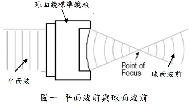
When light waves propagate in space, they have the phenomenon of electromagnetic fluctuations, and the surface of the same phase perpendicular to the continuity of their direction of travel is the wavefront, as shown in Figure 1. Wavefront is one of the most important quality parameters in optical inspection. The quality of optical components and systems is usually measured in terms of wavefront. Wavefront accuracy is closely related to the quality of optical components and system imaging, be it filters, CD/DVD optical readers or digital cameras, wavefront accuracy measurement is the most direct method. Since the optimal wavefront of an optical system is the spherical wavefront, an error of 5 degrees from the spherical wavefront is the wavefront error of the optical system, which can generally be expressed by the Zernike ascending scale or Seidal function. In addition, the measurement of optical components, such as filters, spatial filters and window lenses, is usually based on the measurement of the plano wavefront, which generally requires the beam to change within 1-2 interfering streak errors after passing through the optical components.
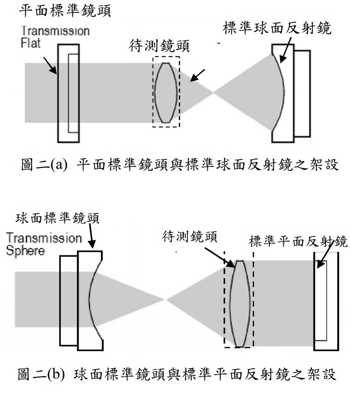
Since the wavefront error tolerance of the optical system is very small, the measurement of wavefront error is almost always detected using an interferometer. As shown in Figure 2, for general optical lenses, two types of setups can be used. In Figure 2(a), using the plane standard lens (optical plate) and the standard spherical reflector, when the plane wavefront passes through the optical lens, it becomes an approximate spherical wavefront, then reflected by the standard spherical reflector, and find the original optical path back to interfere with the plane wavefront in the interferometer, you can detect the wavefront error. It is worth noting that the measured wavefront error is twice the actual value, as the beam goes back through the optical lens twice. In Figure 2(b), the measurement results of the spherical standard lens (transmission sphere) and the standard plane reflector are the same as those assumed in (a). Commercial optical lenses, such as those for digital cameras and projectors, generally require a wavefront error of less than l/4 (l=632.8nm) in order to achieve the image clarity required for basic imaging.
In the international ISO 10110-14 optical standard, the wavefront error is divided into waveform error (P-to-V) and waveform roughness (RMS) in the same way as the surface accuracy of the ISO 10110-5 components, and the wavefront accuracy of general commercial optical lenses is about l/4 waveform error and l/20 waveform roughness. See ISO 10110 optical standard for the relevant measurement markings.
IV. Findings and discussion
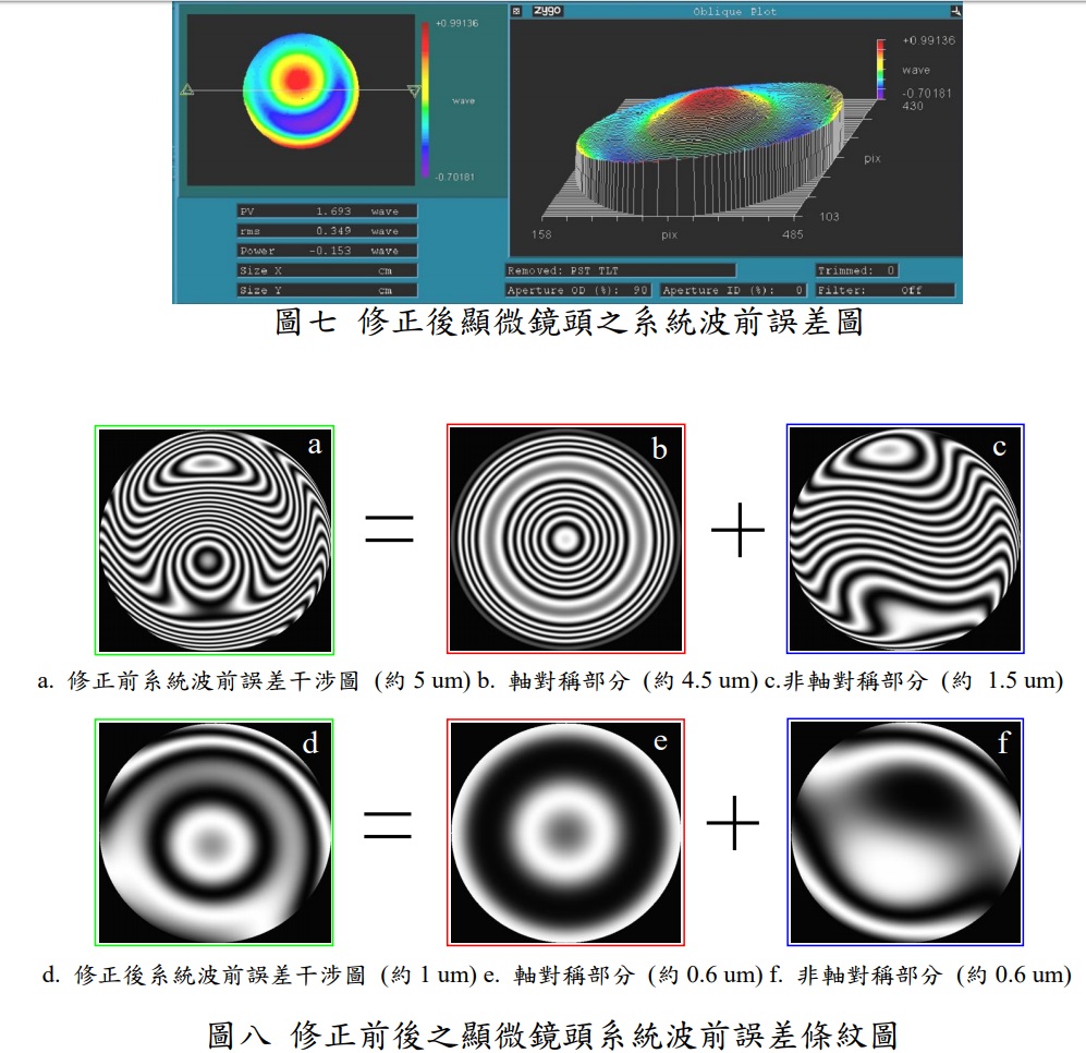
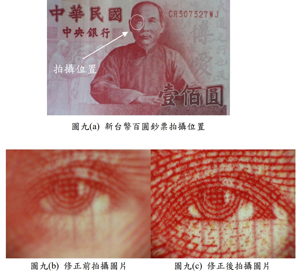
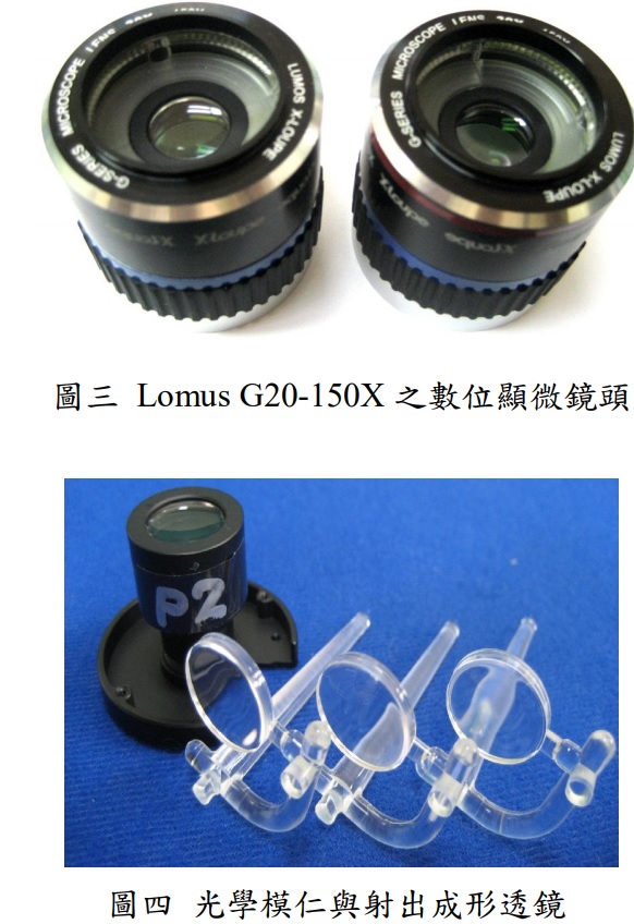
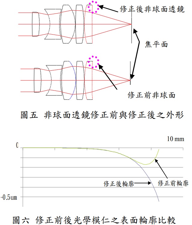
The self-compensating optical die kernel shape correction method uses a 150X microscopic lens as the target optical system (Fig. 3), and a PMMA aspheric plastic lens is used as the lens in front of the optical system to measure the system wavefront error. The PMMA aspheric mirror of the original design microscope was produced by an injection molding machine (Fig. 4) and assembled in the system. The wavefront error of the system was measured by a Fizeau interferometer, and then the wavefront error was input into the optical software. Comparing the shape design values before and after optimization, the die kernel has an external shape correction value of 0.56um, as shown in Figure 6. The aspheric lens made from the post-molded kernel was assembled in the microscopic lens, and the pre-wavelength error of 1.0um (1.65× wavelength) could be measured using an interferometer, as shown in Figure 7. If you compare the wavefront error of the microscopic lens before and after lens correction (as shown in Figure 8), the wavefront error can be reduced from 5um to 1um, and the image taken is the right eye of a portrait of a Taiwan dollar bill, as shown in Figure 9(a). The picture taken by PMMA aspherical lens with the original design microscope, as shown in Figure 9(b), is blurred due to the warpage and shrinkage of the injection molding lens and other production and assembly errors of the lens, making it impossible to obtain clear images. After the die shape correction of PMMA aspheric lens is performed by the self-compensating die shape correction technique, the image obtained, as shown in Figure 9(c), can show the ink details of the banknote clearly, showing that the self-compensating die shape correction has effectively eliminated the production error of the injection molding lens and other errors of the lens.
V. Conclusions and recommendations
The self-compensating die shape correction technique mainly uses the measured system wavefront error to input into the optical design software in the reverse direction for the secondary optimization of the standard component shape. Since the procedure of lens forming and lens system assembly is the same in both cases, all the forming and assembly errors will cancel each other out and the corrected lens shape will directly contribute to the adjustment of the system wavefront error, so this correction technique can be called "Self-compensating optical die shape correction technique". In the future, Multi-field-of-view (MFOV) wavefront error compensation can also be used to cover the system aberration caused by assembly errors in the die shape.